Roeffaers Lab
Nanoscopy and catalysis
Perovskite-based materials for more efficient solar cells
CONTROL OF TEXTURE FORMATION IN PEROVSKITE-BASED MATERIALS FOR MORE EFFICIENT SOLAR CELLS


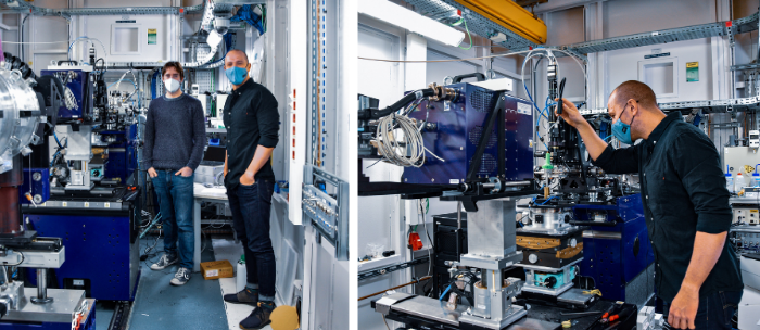
Figure. Eduardo Solano (left), ALBA Synchrotron; and Julian A. Steele (right), KU Leuven; inside the experimental hutch of the NCD-SWEET beamline at the ALBA Synchrotron.
Cerdanyola del Vallès, 10 March 2021. Organic-inorganic metal halide perovskites have undergone a recent revival in the past 10 or so years, most notably being applied to high-efficiency solar cells. This has launched a whole new era of low-cost and high-performing optoelectronic device research, based on cheap, performant materials.
Most optical devices, ranging from LEDs to solar cells, are made up of polycrystalline metal halide perovskite thin films formed by a network of small individual grains with a size of less than 1 micron. Typically, each grain is independent and able to direct its crystal orientation in any direction, giving rise to a random distribution at the macroscale. The basis of current research trends is in locating and controlling spatial heterogeneity across the network of fine grains in order to reduce efficiency losses in these devices.
A promising subfamily of the halide perovskites are the all-inorganic materials, with a composition spanning CsPbI3-xBrx. In these compounds, Iodine (I) is systematically swapped with Bromine (Br) in cesium lead triiodide (CsPbI3), which is the parent material. In order to be developed into functional films, high-temperature processing is required. After thermally processing, the distribution of grain orientations is notably non-random with grains coordinating to align in common directions. This property is called “texture”.
In a recent publication in Advanced Materials, a team of scientists from KU Leuven in Belgium has shown that, in contrast to relatively uninfluential factors like the choice of substrate, film thickness and annealing temperature, Br incorporation modifies the crystal structure by changing the symmetry of the lattice. This change, in turn, governs the formation of the different, energetically favored textures within polycrystalline CsPbI3-xBrx thin films.
The length at which electrons/holes - charge carriers - transport through the films is called carrier diffusion length. Lead halide perovskite semiconductors are known to have long carrier diffusion lengths, which gives rise to high-quality optoelectronic performance, and thus, makes them strong candidates to be used as the light-absorbing layer within solar cells. Consequently, the length scales of carrier diffusion are much longer than a single grain, meaning that long-range mesostructure imposed by texture formation becomes important.
Only with precise statistical data, can the influence of the texture on carrier diffusion and transport within thin films be accurately quantified or understood, leading to improved device performance. Moreover, being able to fine-tune energetically favored polycrystalline texture formations over others will directly influence the potential success of devices made from these materials.

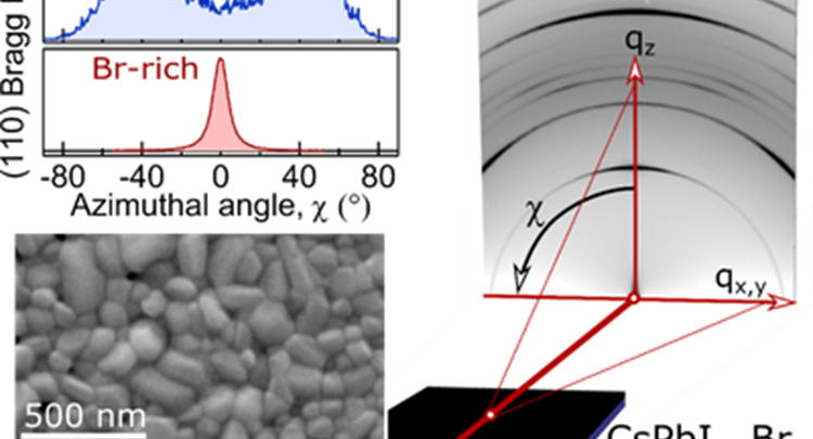
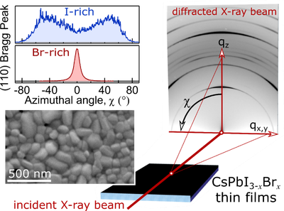
Figure. Schematic of a halide perovskite thin-film comprised of nanograins being measured in a grazing incident wide-angle X-ray scattering (GIWAXS) geometry using synchrotron radiation. The azimuthal plots show two different texture formations (e.g. the direction and distribution of certain crystal planes), depending on Br content.
Need for synchrotron light and large area detection
This is not the first time this research team has come to the ALBA Synchrotron. In a previous work, for which they also made some experiments at the NCD-SWEET beamline, they developed a method to stabilize black CsPbI3 perovskite thin films (the black form is the only optically active) over a glass substrate.
Rapid, large area X-ray detection constitutes one of the only conceivable methods available to fully visualize the structural dynamics and evolution of texture and subtle phase distortions within the black perovskite motifs of CsPbI3-xBrx.
To this aim, the team performed X-Ray Diffraction (XRD) experiments at the Swiss-Norwegian beamlines in the European Synchrotron Radiation Facility (ESRF) in Grenoble and Grazing Incident Wide Angle X-ray Scattering (GIWAXS) experiments at the NCD-SWEET beamline in the ALBA Synchrotron.
Specifically, GIWAXS requires a large area detector, coupled to a bright X-ray source. This allows the evaluation of large scattering angle ranges in one quick exposure.
As explained by Julian A. Steele, first author of the publication: “Beyond the high-resolution diffraction pattern used to identify lattice distortions, the high-throughput capabilities at the NCD-SWEET beamline allowed a large parameter space to be explored with ease: parameters like material thickness and composition, choice of different functional device layers, processing temperature... You can see how such a parameter space explodes rapidly once all of the important factors are considered, and the facilities provided at ALBA allowed us to manage to handle this well.”
Most significantly, the findings described in this work unlock the interpretation of several anomalous reports of anisotropic thin-film behavior, typically generated by other groups using linear or single-pixel X-ray scattering detection, which are usually routine in-house instruments.
“Comparing our findings to the wider research on hybrid organic-inorganic halide perovskites, the insights revealed here using synchrotron GIWAXS unify all other previous texture observations.” Says Steele.
This work has involved contributions from several international research laboratories: the KU Leuven and Ghent University in Belgium, the ALBA Synchrotron in Spain, the European Synchrotron Radiation Facility (ESRF) in France, the Lawrence Berkeley National Laboratory and the University of California, Berkeley in the USA, the Helmholtz-Zentrum Berlin für Materialien und Energie and the Max Plank Institute for Polymer Research in Germany, and EDAX (Ametek BV) in the Netherlands.
Reference: Julian A. Steele, Eduardo Solano, Handong Jin, Vittal Prakasam, Tom Braeckevelt, Haifeng Yuan, Zhenni Lin, René de Kloe, Qiong Wang, Sven M. J. Rogge, Veronique Van Speybroeck, Dmitry Chernyshov, Johan Hofkens, and Maarten B. J. Roeffaers. Texture Formation in Polycrystalline Thin Films of All-Inorganic Lead Halide Perovskite. Adv. Mater. 2021, 2007224. DOI: 10.1002/adma.202007224
To enable comments sign up for a Disqus account and enter your Disqus shortname in the Articulate node settings.